Shattering the AI Memory Wall: NEO Semiconductor Debuts NEO.AI as Atomically Thin 2D Chips Redefine Computing Limits
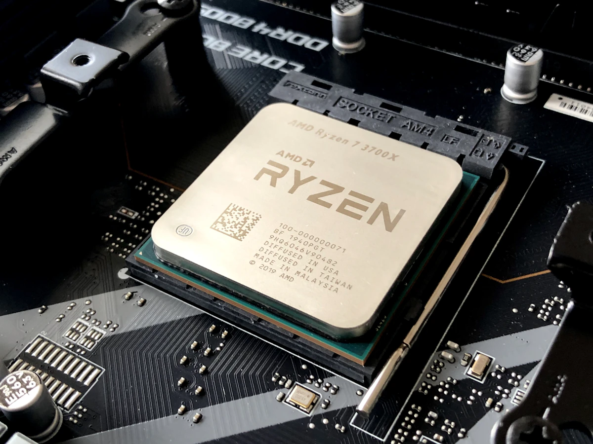
Featured Asset: Next-Generation Silicon Wafer and High-Density AI Microchip Architecture
Executive Summary
On August 4, 2026, the semiconductor industry took a monumental step toward breaking the "AI Memory Wall." At the Future of Memory and Storage (FMS 2026) conference in Santa Clara, NEO Semiconductor officially launched its NEO.AI platform, featuring X-SRAM (delivering up to 5× higher on-chip cache density) and 3D X-DRAM (enabling up to 10× higher HBM capacity). Simultaneously, material scientists debuted an atomically thin 2D flash memory chip built with $MoS_2$, paving the way for ultra-fast, energy-efficient in-memory computing.
1. NEO Semiconductor Launches NEO.AI to Solve AI's Greatest Bottlenecks
As frontier artificial intelligence models scale past trillions of parameters, processing speed is increasingly constrained not by raw compute power, but by the AI Memory Wall—the physical speed and capacity limits of transferring data between GPUs and onboard memory.
At FMS 2026 on August 4, NEO Semiconductor introduced a unified architecture designed to eliminate these bottlenecks. The platform integrates two core innovations:
- X-SRAM (On-Chip AI Cache): Delivers up to 5× higher memory density than conventional SRAM while maintaining full compatibility with standard CMOS nanosheet manufacturing processes.
- 3D X-DRAM (High Bandwidth Memory): Utilizes proven 3D NAND manufacturing techniques to scale HBM memory capacity by up to 10×, dramatically boosting GPU utilization for multi-trillion parameter MoE models.

Figure 1: High-density 3D stacked memory architectures optimizing bandwidth for enterprise AI clusters.
2. Atomically Thin 2D Memory Chips Redefine In-Memory Search Operations
In parallel hardware research, materials scientists revealed on August 4, 2026, an experimental analogue Content-Addressable Memory (CAM) array built using atomically thin two-dimensional Molybdenum Disulfide ($MoS_2$) flash memory cells.
By pairing $MoS_2$ monolayers with semimetal antimony ($Sb$) contacts, the chip achieves ultra-fast, energy-efficient in-memory search operations at atomic dimensions. This architecture enables analog computing directly inside the memory array, reducing data transfer latency and power consumption by up to 80% compared to silicon-based designs.

Figure 2: Cleanroom semiconductor fabrication processes adapting to 2D material integration and 3D stacking.
3. Venture Capital and Custom Silicon Investments Soar in August 2026
The hardware breakthrough coincides with massive capital infusion into custom silicon startups. On August 3, UK-based custom AI chip startup Olix closed a $312 million Series B round at a $3.3 billion valuation, highlighting growing investor confidence in alternative accelerator architectures designed to challenge dominant GPU monoliths.
Key Takeaways for Hardware Architects & Developers
- Overcoming On-Chip Caching Limits: Monolithic 3D SRAM scaling allows larger context windows to remain directly on the processor die for zero-latency inference.
- 3D DRAM Manufacturing Scaling: Adapting mature 3D NAND vertical structures to DRAM significantly lowers high-capacity HBM production costs.
- In-Memory Computing Emergence: 2D sub-nanometer materials enable localized tensor calculations, paving the way for low-power edge AI deployments.

Comments
Post a Comment